A transistor is a semiconductor, meaning that sometimes it conducts electricity, and sometimes it doesn’t. Its internal resistance varies, depending on the power that you apply to its base.
NPN and PNP transistors are bipolar semiconductors. They contain two slightly different variants of silicon, and conduct using both polarities of carriers-holes and electrons.
The NPN type is a sandwich with P-type silicon in the middle, and the PNP type is a sandwich with N-type silicon in the middle. if you want to know more about this terminology and the behavior of electrons when they try to cross an NP junction or a PN junction.
1. All bipolar transistors have three connections: Collector, Base, and Emitter, abbreviated as C, B, and E on the manufacturer’s data sheet, which will identify the pins for you.
2. NPN transistors are activated by positive voltage on the base relative to the emitter.
3. PNP transistors are activated by negative voltage on the base relative to the emitter.
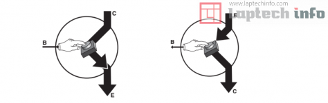
You can think of a bipolar transistor as if it contains a little button inside, as shown in two photos below. When the button is pressed, it allows a large current to flow. To press the button, you inject a much smaller current into the base by applying a small voltage to the base. In an NPN transistor, the control voltage is positive, in a PNP transistor, the control voltage is negative.

NPN transistor:
- To start the flow of current from collector to emitter, apply a relatively positive voltage to the base.
- In the schematic symbol, the arrow points from base to emitter and shows the direction of positive current.
- The base must be at least 0.6 volts "more positive" than the emitter, to start the flow.
- The collector must be "more positive" than the emitter.
PNP transistor:.
- To start the flow of current from emitter to collector, apply a relatively negative voltage to the base.
- In the schematic symbol, the arrow points from emitter to base and shows the direction of positive current.
- The base must be at least 0.6 volts "more negative" than the emitter, to start the flow.
- The emitter must be "more positive" than the collector.

NPN and PNP transistors are bipolar semiconductors. They contain two slightly different variants of silicon, and conduct using both polarities of carriers-holes and electrons.
The NPN type is a sandwich with P-type silicon in the middle, and the PNP type is a sandwich with N-type silicon in the middle. if you want to know more about this terminology and the behavior of electrons when they try to cross an NP junction or a PN junction.
1. All bipolar transistors have three connections: Collector, Base, and Emitter, abbreviated as C, B, and E on the manufacturer’s data sheet, which will identify the pins for you.
2. NPN transistors are activated by positive voltage on the base relative to the emitter.
3. PNP transistors are activated by negative voltage on the base relative to the emitter.
You can think of a bipolar transistor as if it contains a little button inside, as shown in two photos below. When the button is pressed, it allows a large current to flow. To press the button, you inject a much smaller current into the base by applying a small voltage to the base. In an NPN transistor, the control voltage is positive, in a PNP transistor, the control voltage is negative.
NPN transistor:
- To start the flow of current from collector to emitter, apply a relatively positive voltage to the base.
- In the schematic symbol, the arrow points from base to emitter and shows the direction of positive current.
- The base must be at least 0.6 volts "more positive" than the emitter, to start the flow.
- The collector must be "more positive" than the emitter.
PNP transistor:.
- To start the flow of current from emitter to collector, apply a relatively negative voltage to the base.
- In the schematic symbol, the arrow points from emitter to base and shows the direction of positive current.
- The base must be at least 0.6 volts "more negative" than the emitter, to start the flow.
- The emitter must be "more positive" than the collector.